|
Feature:
|
|
Capacity
|
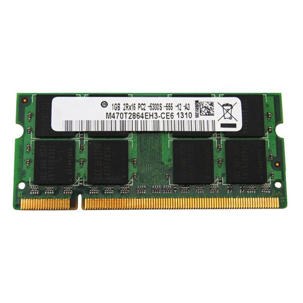
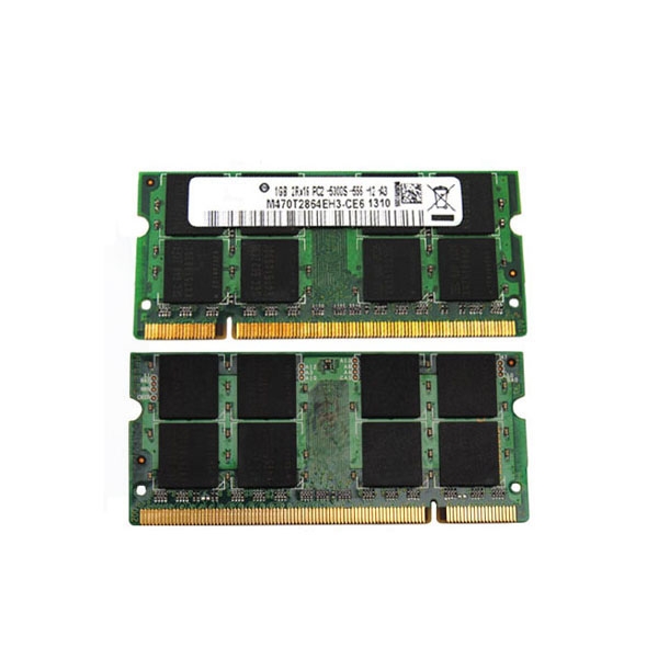
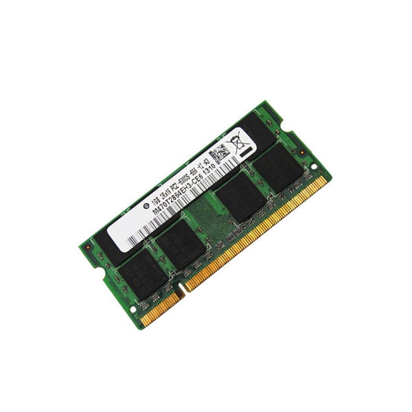
1GB/2GB/4GB DDR2 RAM
|
|
DDR Memory Type
|
DDR2
|
|
No. of Pins
|
204 Pin
|
|
Memory Speed MHz
|
533/667/800MHZ
|
|
Module Type
|
SO DIMM
|
|
Function
|
Non ECC Memory
|
|
|
|
Detail Description:
|
|
1) DDRII 533/667/800 MHz
|
|
2) 168/184/240-pin socket type dual in line memory module (DIMM)
|
|
3) 2.6V power supply
|
|
4) Data rate: 533/667/800Mbps (max.)
|
|
5) 2.5 V (SSTL-2 compatible) I/O for DDR I products,1.8Vpower supply for DDR II products
|
|
6) Double-data-rate architecture, two data transfers per clock cycle
|
|
7) Bi-directional, differential data strobe (DQS) is transmitted/received with data, to be used in capturing data at the receiver
|
|
8) Data inputs and outputs are synchronized with DQS
|
|
9) DQS is edge aligned with data for read, center aligned with data for write
|
|
10) Differential clock inputs (CK and CK)
|
|
11) DLL aligns DQ and DQS transitions with CK transitions
|
|
12) Commands entered on each positive CK edge: data and data mask referenced to both edges of DQS
|
|
13) Four internal banks for concurrent operation (component)
|
|
14) Data mask(DM) for write data
|
|
15) Auto precharge option for each burst access
|
|
16) Programmable burst length: 2, 4, 8
|
|
17) Programmable/CAS latency (CL): 3
|
|
18) Programmable output driver strength: normal/weak
|
|
19) Refresh cycles: (8192 refresh cycles/64ms)
|
|
20) 7.8US maximum average periodic refresh interval
|
|
21) Posted CAS by programmable additive latency for better command and data bus efficiency
|
|
22) Off-chip-driver impedance adjustment and on-die-termination for better signal quality
|
|
23) DQS can be disabled for single-ended data strobe operation
|
|
24) 2 variations of refresh
|
|
25) Auto refresh
|